Hauptinhalt
2024
Inhalt ausklappen Inhalt einklappen J. Phys. Chem. C.: "Two Isomeric Thienoacenes in Thin Films: Unveiling the Influence of Molecular Structure and Intermolecular Packing on Electronic Properties

Ch. Gatsios, M. Dreher, P. Amsalem, A. Opitz, R. Jouclas, Y. Geerts, G. Witte, N. Koch
J. Phys. Chem. C.,128, 21228 - 21236 (2024), • DOI: 10.1021/acs.jpcc.4c06741
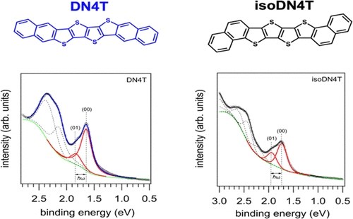
Isomerism of molecular structures is often encountered in the field of organic semiconductors, but little is known about how it can impact electronic and charge transport properties in thin films. This study reveals the molecular orientation, electronic structure, and intermolecular interactions of two isomeric thienoacenes (DN4T and isoDN4T) in thin films, in relation to their charge transport properties. Utilizing scanning tunneling microscopy (STM), angle-resolved photoemission spectroscopy (ARUPS), and near-edge X-ray absorption fine structure measurements (NEXAFS), we systematically analyze the behavior of these isomers from submonolayer to multilayer coverage on highly ordered pyrolytic graphite (HOPG) as substrates. We find that at submonolayer coverage both DN4T and isoDN4T molecules predominantly adopt a nearly flat-lying orientation on the surface, minimizing intermolecular interactions. The distinct emission features of the highest occupied molecular orbital (HOMO) level in ARUPS enables the determination of molecular reorganization energies. These are found to be in good agreement with theoretical predictions, suggesting superior charge transport in DN4T compared to isoDN4T. Notably, thickness-dependent photoemission measurements reveal a significant splitting (approximately 450 meV) of the HOMO level of isoDN4T, attributed to polarization-induced effects rather than wave function overlap, indicating a nuanced interplay between molecular packing and electronic properties. Our results underscore the importance of molecular packing and substrate interactions in determining the electronic structure and transport properties of organic semiconductor thin films. Substrate-induced polymorphism and the crucial role of polarization-induced effects influencing charge transport are highlighted. These insights are pivotal for future engineering of molecular and thin film structures, aiming to enhance the performance of organic semiconductor-based devices.Inhalt ausklappen Inhalt einklappen J. Phys. Chem. Lett.: "Ultrafast Time-Domain Spectroscopy Reveals Coherent Vibronic Couplings upon Electronic Excitation in Crystalline Organic Thin Films"

S. Souri, D. Timmer, D. C. Lünemann, N. Hadilou, K. Winte, A. De Sio, M. Esmann, F. Curdt, M. Winklhofer, S. Anhäuser, M. Guerrini, A. M. Valencia, C. Cocchi, G. Witte, C. Lienau
J. Phys. Chem. Lett., 15, 11170−11181 (2024), • DOI: 10.1021/acs.jpclett.4c02711
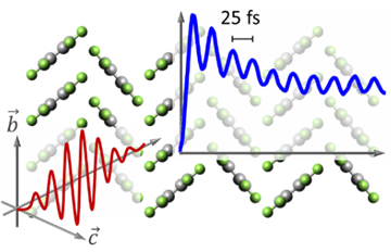
The coherent coupling between electronic excitations and vibrational modes of molecules largely affects the optical and charge transport properties of organic semiconductors and molecular solids. To analyze these couplings by means of ultrafast spectroscopy, highly ordered crystalline films with large domains are particularly suitable because the domains can be addressed individually, hence allowing azimuthal polarization-resolved measurements. Impressive examples of this are highly ordered crystalline thin films of perfluoropentacene (PFP) molecules, which adopt different molecular orientations on different alkali halide substrates. Here, we report polarization-resolved time-domain vibrational spectroscopy with 10 fs time resolution and Raman spectroscopy of crystalline PFP thin films grown on NaF(100) and KCl(100) substrates. Coherent oscillations in the time-resolved spectra reveal vibronic coupling to a high-frequency, 25 fs, in-plane deformation mode that is insensitive to the optical polarization, while the coupling to a lower-frequency, 85 fs, out-of-plane ring bending mode depends significantly on the crystalline and molecular orientation. Comparison with calculated Raman spectra of isolated PFP molecules in vacuo supports this interpretation and indicates a dominant role of solid-state effects in the vibronic properties of these materials. Our results represent a first step toward uncovering the role of anisotropic vibronic couplings for singlet fission processes in crystalline molecular thin films.Inhalt ausklappen Inhalt einklappen Nanoscale: "Transport, trapping, triplet fusion: thermallyretarded exciton migration in tetracene single crystals"

Dominik Muth, Sebastian Anhäuser, Daniel Bischof, Anton Krüger, Gregor Witte and Marina Gerhard
Nanoscale, 16, 13471-13482 (2024), • DOI: 10.1039/d4nr01086h
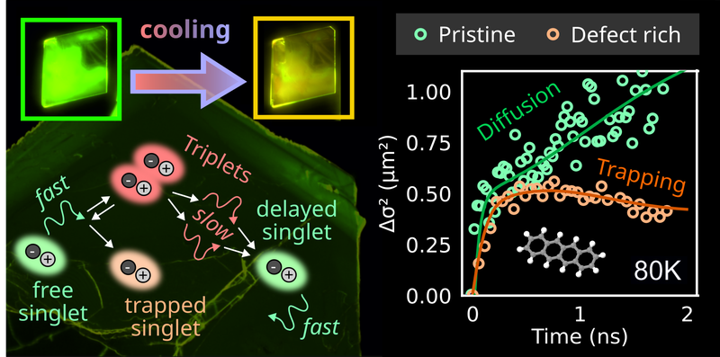
Efficient exciton migration is crucial for optoelectronic organic devices. While the transport of triplet excitons is generally slow compared to singlet excitons, triplet exciton migration in certain molecular semiconductors with endothermic singlet fission appears to be enhanced by a time-delayed regeneration of the more mobile singlet species via triplet fusion. This combined transport mechanism could be exploited for devices, but the interplay between singlet fission and triplet fusion, as well as the role of trap states is not yet well understood. Here, we study the spatiotemporal exciton dynamics in the singlet fission material tetracene by means of time resolved photoluminescence micro-spectroscopy on crystalline samples of different quality. Varying the temperature allows us to modify the dynamic equilibrium between singlet, triplet and trapped excitons. Supported by a kinetic model, we find that thermally activated dissociation of triplet pairs into free triplet excitons can account for an increase of the diffusion length below room temperature. Moreover, we demonstrate that trapping competes efficiently with exciton migration.Inhalt ausklappen Inhalt einklappen ACS Appl. Mater. Interfaces: "Heteroepitaxy in Organic/TMD Hybrids and Challenge to Achieve it for TMD Monolayers: The Case of Pentacene on WS2 and WSe2"

D. Günder, M. Axt, and G. Witte
ACS Appl. Mater. Interfaces, 16, 1911−1920 (2024), • DOI: 10.1021/acsami.3c15829
The intriguing photophysical properties of monolayer stacks of different transition-metal dichalcogenides (TMDs), revealing rich exciton physics including interfacial and moiré excitons, have recently prompted an extension of similar investigations to hybrid systems of TMDs and organic films, as the latter combine large photoabsorption cross sections with the ability to tailor energy levels by targeted synthesis. To go beyond single-molecule photoexcitations and exploit the excitonic signatures of organic solids, crystalline molecular films are required. Moreover, a defined registry on the substrate, ideally an epitaxy, is desirable to also achieve an excitonic coupling in momentum space. This poses a certain challenge as excitonic dipole moments of organic films are closely related to the molecular orientation and film structure, which critically depend on the support roughness. Using X-ray diffraction, optical polarization, and atomic force microscopy, we analyzed the structure of pentacene (PEN) multilayer films grown on WSe2(001) and WS2(001) and identified an epitaxial alignment. While (022)-oriented PEN films are formed on both substrates, their azimuthal orientations are quite different, showing an alignment of the molecular L-axis along the ⟨110⟩WSe2 and ⟨100⟩WS2 directions. This intrinsic epitaxial PEN growth depends, however, sensitively on the substrates surface quality. While it occurs on exfoliated TMD single crystals and multilayer flakes, it is hardly found on exfoliated monolayers, which often exhibit bubbles and wrinkles. This enhances the surface roughness and results in (001)-oriented PEN films with upright molecular orientation but without any azimuthal alignment. However, monolayer flakes can be smoothed by AFM operated in contact mode or by transferring to ultrasmooth substrates such as hBN, which again yields epitaxial PEN films. As different PEN orientations result in different characteristic film morphologies (elongated mesa islands vs pyramidal dendrites), which can be easily distinguished by AFM or optical microscopy, this provides a simple means to judge the roughness of the used TMD surface.