Main Content
Research Topics
What actually makes a good solar cell? Or a bad one? How does sunlight turn into charge carriers and how do charge carriers become usable electricity? The processes that are crucial for answering such questions take place on very short time scales, often shorter than a nanosecond. To get to the bottom of things, we work with femtosecond laser pulses to optically excite semiconductor materials and we study the luminescence emitted during the transition back to the ground state. The time decay of the luminescence signal tells us a lot - for example, about the transport of charge carriers or bound electron-hole pairs, so-called excitons, about the properties of internal interfaces, or about the presence of defect states. Overall, our intention is to better understand how the micro- and nanostructure or the nature of interfaces affect the optical properties of organic and organic/inorganic semiconductor devices. We are particularly interested in these systems:
· Molecular single crystals and thin films
· Hybrid organic/inorganic materials
· Organic/organic and organic/inorganic heterostructures
Fundamental processes in molecular semiconductors
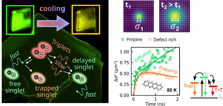
Unlike inorganic semiconductors, organic semiconductors are not held together by electronic bonds, but rather by comparatively weak van-der-Waals interactions between the molecular building blocks. This has significant effects on the resulting band structure, optical properties and the transport of charge carriers or excitons. Two well-known phenomena are particularly noteworthy here, namely the spin-allowed splitting of a singlet exciton into two triplet excitons or the formation of so-called excimers through the structural relaxation of excited molecules. These processes can compete with each other and may be desirable or undesirable depending on the application. Fundamental investigations of the relationship between the packing motif, the optical properties and the dynamics of optical excitations are therefore crucial for the development of theoretical models with high predictive power.

For further reading:
D. Muth et al., „Transport, trapping, triplet fusion: Thermally retarded exciton migration in tetracene single crystals”, Nanoscale 16, 13471 (2024). DOI: 10.1039/D4NR01086H
J. Thompson et al., “Singlet Exciton Optics and Dynamics in Oligoacene Semiconductor Crystals”, Nat. Sci. 3, e20220040 (2023). DOI: 10.1002/admi.202300922
D. Bischof et al., “Regioselective Fluorination of Acenes: Tailoring of Molecular Electronic Levels and Solid State Properties”, Chem. – A Eur. J. 28, e202103653 (2022). DOI: 10.1002/chem.202103653
Hybrid materials
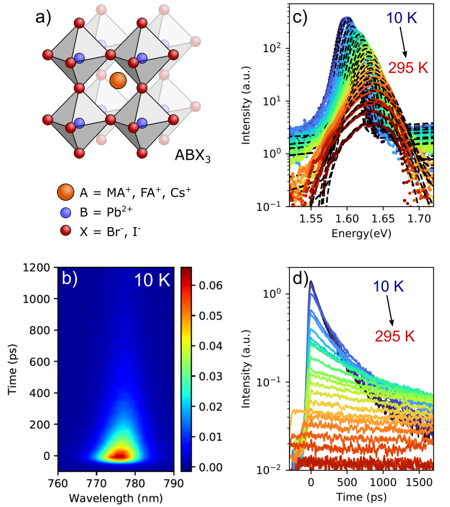
The combination of organic and inorganic materials, for example in the form of adamantane-like cluster compounds or hybrid perovskite semiconductors, makes it possible to adjust the optical properties over a wide range by selectively varying the organic and inorganic components. The strong electron-phonon coupling in these systems sometimes leads to a strong localization of optical excitations in the form of excimers or polarons, which significantly influence the resulting properties.

For further reading:
F. Schmitz et al., ”Tuning the Optical Properties of 2D Monolayer Silver-Bismuth Bromide Double Perovskite by Halide Substitution“, Nanotechnology 33, 215706 (2022). DOI: 10.1088/1361-6528/ac54df
E. Geringer et al., “Introducing Distinct Structural and Optical Properties into Organotin Sulfide Clusters by the Attachment of Perylenyl and Corannulenyl Groups”, Inorg. Chem. 60, 19381 (2021). DOI: 10.1021/acs.inorgchem.1c03206
E. Geringer et al., “Pyrene-Terminated Tin Sulfide Clusters: Optical Properties and Deposition on a Metal Surface”, Chem. Eur. J. 27, 2734 (2021). DOI: 10.1002/chem.202003889
Excitation dynamics in semiconductor heterostructures
When two different semiconductor materials are brought together, many new questions arise with regard to the interface. Can excitations migrate from one material to the other? Are charges separated at the interface? Do we perhaps observe new signatures in optical spectra that can be assigned to the interface? And what do such signatures reveal about the nature of the interface? Addressing such questions is crucial for assessing the potential of new materials for semiconductor devices. Depending on the electronic structure at the interface, a distinction is made between type-I-heterojunctions, which enable a transfer of excitation energy from one material to another, and type-II-heterojunctions, where charges are separated from each other.

For further reading:
N. Hofeditz et al., ”Efficient Energy Transfer and Singlet Fission in Co-Deposited Thin Films of Pentacene and Anthradithiophene”, Adv. Mater. Interfaces 11, 2300922 (2024). DOI: 10.1002/admi.202300922
N. Hofeditz et al., “Photoexcitation Dynamics in Strongly Interacting Donor/Acceptor Blends Probed by Time-Resolved Photoluminescence Spectroscopy”, J. Phys. Chem. C 125, 17194 (2021). DOI: 10.1021/acs.jpcc.1c04183
M. Gerhard et al., “Field-induced exciton dissociation in PTB7-based organic solar cells”, Phys. Rev. B 95, 195301 (2017). DOI: 10.1103/PhysRevB.95.195301
Defects and disorder
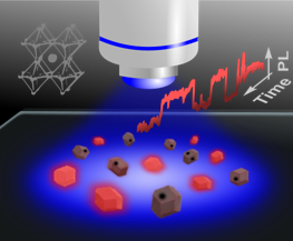
Semiconductors are not perfect. Structural disorder or defects can strongly influence and impair the opto-electronic properties. Luminescence spectroscopy is particularly sensitive to the effects of defects and composition-related disorder as it reveals non-radiative processes or the signatures of defects in low temperature spectra. Of particular interest here is the relationship between the luminescence properties and the micro- or nanostructure of a semiconductor sample.

For further reading:
M. Gerhard et al., “Heterogeneities and Emissive Defects in MAPbI3 Perovskite Revealed by Spectrally Resolved Luminescence Blinking”, Adv. Opt. Mater. 9, 2001380 (2021). DOI: 10.1002/adom.202001380
M. Gerhard et al., “Microscopic Insight into Non-Radiative Decay in Perovskite Semiconductors from Temperature-Dependent Luminescence Blinking”, Nat. Commun. 10, 1698 (2019). DOI: 10.1038/s41467-019-09640-w